
Welcome to the definitive guide on a career that sits at the very heart of modern technological innovation. If you've ever been fascinated by the magic that happens inside a microchip, wondered how self-driving cars perceive the world in real-time, or considered a career that blends the logic of software with the tangible impact of hardware, you've arrived at the right place. The role of an FPGA Engineer is one of the most dynamic, challenging, and financially rewarding paths in the engineering world.
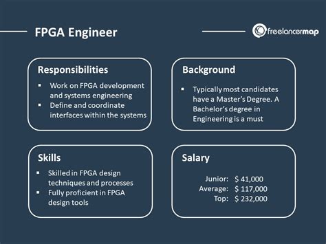
This career is not just about a job; it's about becoming an architect of the digital age. FPGA engineers are the wizards who program hardware itself, creating custom circuits for everything from 5G base stations and data center accelerators to advanced medical imaging devices and spacecraft. The demand for this unique skill set is soaring, and with it, the FPGA engineer salary has become one of the most competitive in the tech industry, with average compensation packages often ranging from a strong $110,000 to well over $220,000 per year, depending on a variety of factors we will explore in detail.
As a career analyst who has guided numerous hardware engineers through their professional journeys, I've seen firsthand the transformative power of this role. I once mentored a recent graduate who was passionate but intimidated by the field. Two years later, he sent me a photo of a commercial satellite communication product on the market. He proudly pointed to a specific component and said, "My verification module runs right there, ensuring every data packet is perfect. I helped build a piece of the future." It’s this direct, tangible impact on cutting-edge technology that makes an FPGA career so compelling.
This guide is designed to be your comprehensive roadmap. We will dissect every component of an FPGA engineer's salary, explore the factors that can maximize your earning potential, and provide a step-by-step plan to launch or advance your career in this exciting field.
### Table of Contents
- [What Does an FPGA Engineer Do?](#what-does-an-fpga-engineer-do)
- [Average FPGA Engineer Salary: A Deep Dive](#average-fpga-engineer-salary-a-deep-dive)
- [Key Factors That Influence Salary](#key-factors-that-influence-salary)
- [Job Outlook and Career Growth](#job-outlook-and-career-growth)
- [How to Get Started in This Career](#how-to-get-started-in-this-career)
- [Conclusion: Is an FPGA Career Right for You?](#conclusion-is-an-fpga-career-right-for-you)
What Does an FPGA Engineer Do?
Before we dive into the numbers, it's crucial to understand the intricate and fascinating work that justifies such a strong salary. An FPGA, or Field-Programmable Gate Array, is a special type of integrated circuit. Think of a standard processor (CPU) as a factory with a fixed assembly line, designed to perform a wide range of tasks sequentially but with a set structure. An FPGA, in contrast, is like a warehouse full of programmable logic blocks and interconnects—a blank slate. An FPGA Engineer is the architect who designs and builds a custom, hyper-efficient assembly line within that warehouse, specifically tailored for one particular task.
This process is fundamentally different from software programming. While a software engineer writes instructions for a fixed processor, an FPGA engineer uses a Hardware Description Language (HDL), such as Verilog or VHDL, to describe the physical digital circuits. This code doesn't just run *on* the chip; it *defines* the chip's structure. The result is a hardware implementation that can perform tasks with incredible speed and parallelism, far surpassing what's possible with a general-purpose CPU for certain applications.
Core Responsibilities and Daily Tasks:
An FPGA Engineer's work spans the entire design lifecycle, from concept to in-system validation. Their daily routine is a blend of creative design, rigorous analysis, and hands-on testing.
- Requirements and Architecture: Collaborating with system architects and other engineers to understand the project goals and define the functional requirements for the FPGA. This involves deciding what tasks the FPGA will handle, its performance targets, and how it will interface with the rest of the system.
- RTL Design and Coding: This is the core creative process. Using Verilog or SystemVerilog, the engineer writes Register-Transfer Level (RTL) code that describes the desired digital logic—state machines, data paths, control units, and more. This requires a deep understanding of digital logic design principles.
- Simulation and Verification: Before a design is ever programmed onto a physical chip, it must be exhaustively tested in a simulated environment. The engineer writes testbenches (often using advanced methodologies like UVM) to create stimuli and check that the RTL code behaves exactly as intended under all possible conditions. This phase is critical and often consumes the most time.
- Synthesis, Place & Route (P&R): Once the design is verified, specialized software tools (like AMD/Xilinx Vivado or Intel Quartus) take the RTL code and "synthesize" it into a netlist of logic gates. The tools then "place" these gates onto the physical logic blocks of the FPGA and "route" the connections between them.
- Timing Closure: The engineer must analyze the results of P&R to ensure the design can run at the required clock speed. If signals take too long to travel between logic blocks (a "timing violation"), the engineer must optimize the RTL code or guide the tools to find a better solution. This is one of the most challenging aspects of the job.
- Hardware Bring-Up and Debugging: The finalized design is downloaded onto a physical FPGA on a development board. The engineer then works in the lab with oscilloscopes and logic analyzers to test the design in a real-world system, debugging any issues that weren't caught in simulation.
### A Day in the Life of a Mid-Level FPGA Engineer
To make this more concrete, let's follow "Maria," a mid-level FPGA Engineer at a telecommunications company.
- 9:00 AM - Daily Stand-up: Maria joins her team's brief meeting. She reports that she fixed a critical bug in her 5G data-processing module and will spend today working on meeting the timing constraints for the new 250 MHz clock speed.
- 9:15 AM - RTL Optimization: Back at her desk, Maria analyzes the timing report from last night's automated build. The tool failed to meet the speed requirement. She identifies the critical path in her Verilog code and spends the next couple of hours refactoring the logic, adding pipeline stages to shorten the signal path and reduce delay.
- 11:30 AM - Kicking off a Simulation: After making the code changes, she modifies her SystemVerilog testbench to ensure the new pipelined logic still produces the correct output. She launches a regression simulation on a powerful server farm, which will run for several hours.
- 12:30 PM - Lunch: Maria has lunch with a software engineer and a PCB designer to discuss how the FPGA's new interface will interact with the board's main processor.
- 1:30 PM - Peer Code Review: She spends an hour reviewing a junior engineer's code for a new control register interface, providing feedback on coding style and potential logic errors.
- 2:30 PM - Lab Debugging: Maria heads to the hardware lab. A prototype board is showing intermittent data corruption. She connects a logic analyzer to the FPGA's output pins to capture high-speed signal data, trying to correlate the corruption with other system events.
- 4:30 PM - Analysis and Documentation: Back at her desk, she analyzes the captured data and reviews the simulation results, which have now completed. The simulation passed, confirming her RTL fix was logically correct. She documents her lab findings and her RTL changes in the project's tracking system before running a new synthesis and P&R build overnight.
This example illustrates the multidisciplinary nature of the role—it's a constant cycle of design, verification, and hands-on problem-solving.
Average FPGA Engineer Salary: A Deep Dive
The salary for an FPGA Engineer is a direct reflection of the role's high complexity, the specialized education required, and the immense value it brings to technology companies. Compensation is consistently strong across the board and significantly outpaces many other engineering disciplines.
It's important to note that salary data is dynamic. The figures presented here are based on an aggregation of recent data from 2023 and 2024 from leading compensation platforms and industry analysis.
National Averages and Typical Salary Ranges
Across the United States, the compensation landscape for FPGA engineers is robust. Here’s a summary of what you can expect:
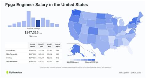
- Overall Average Base Salary: Most reputable sources place the average base salary for an FPGA Engineer in the United States between $125,000 and $145,000 per year.
- Payscale.com reports an average base salary of approximately $123,871, with a typical range from $86,000 to $165,000.
- Glassdoor.com indicates a higher median pay of around $144,250, with a likely range spanning from $113,000 to $184,000.
- Salary.com provides a more granular view for an "FPGA Design Engineer," showing a median salary of $130,401, with the middle 50% of engineers earning between $120,011 and $141,600.
These figures represent the *base salary* only. Total compensation, which includes bonuses, stock awards, and other benefits, can be significantly higher, often pushing senior-level engineers well into the $200,000+ range.
FPGA Engineer Salary by Experience Level
Experience is arguably the single most significant driver of salary growth in this field. As engineers gain expertise in design, verification, and tackling complex timing and architectural challenges, their value skyrockets. The career progression from an entry-level position to a senior or principal role is marked by substantial increases in both responsibility and compensation.
Here is a breakdown of typical salary brackets based on years of experience, synthesizing data from sources like Glassdoor, Payscale, and Levels.fyi (which provides excellent data for high-paying tech companies).
| Experience Level | Typical Years of Experience | Typical Base Salary Range (USD) | Potential Total Compensation (including bonus/stock) |
| :--- | :--- | :--- | :--- |
| Entry-Level FPGA Engineer | 0 - 2 Years | $85,000 - $115,000 | $95,000 - $130,000 |
| Mid-Career FPGA Engineer | 3 - 7 Years | $115,000 - $160,000 | $140,000 - $190,000 |
| Senior FPGA Engineer | 8 - 14 Years | $160,000 - $195,000 | $190,000 - $260,000+ |
| Staff / Principal FPGA Engineer | 15+ Years | $195,000 - $240,000+ | $250,000 - $400,000+ |
*(Note: These are representative ranges for the US market. Top-tier companies in high-cost-of-living areas may exceed these figures significantly.)*
A Closer Look at Compensation Components
An FPGA Engineer's offer letter is more than just a base salary. Understanding the full compensation package is key to evaluating an opportunity.
1. Base Salary: This is the guaranteed, fixed portion of your pay. It forms the foundation of your earnings and is what the figures above primarily represent.
2. Annual Performance Bonus: Most companies offer a cash bonus, typically paid out annually or quarterly. This is often calculated as a percentage of your base salary (e.g., 10-20%) and is tied to both your individual performance and the company's financial success.
3. Stock Awards (RSUs): This is a major wealth-building component, especially at publicly traded tech companies. Restricted Stock Units (RSUs) are grants of company stock that vest (become yours) over a period, typically four years with a one-year "cliff" (meaning you receive the first 25% after your first year). For senior roles at companies like Apple, Google, NVIDIA, or Meta, the annual value of RSU grants can equal or even exceed the base salary.
4. Signing Bonus: A one-time, lump-sum payment offered to new hires as an incentive to join the company. This can range from a few thousand dollars for entry-level roles to over $50,000 for highly sought-after senior engineers.
5. Profit Sharing: Some companies, particularly those that are well-established and consistently profitable, may distribute a portion of their profits to employees. This is less common in the tech startup world but can be a significant benefit at certain industrial or financial firms.
6. Comprehensive Benefits: While not direct cash, the value of benefits is substantial. This includes high-quality health, dental, and vision insurance; a strong 401(k) retirement plan with employer matching; generous paid time off (PTO); parental leave; and professional development budgets. These benefits can easily add another $20,000-$30,000 in effective value to your annual compensation.
When considering an offer, it's essential to look at the Total Compensation (TC)—the sum of base salary, target bonus, and the annualized value of stock grants. This provides a much more accurate picture of your earning potential than base salary alone.
Key Factors That Influence FPGA Engineer Salary

While experience level provides a broad framework for salary expectations, several other critical factors can dramatically influence your earning potential. A strategic understanding of these elements can empower you to negotiate more effectively and guide your career choices toward higher-paying opportunities. This section, the most detailed in our guide, breaks down each of these influential factors.
###
Level of Education
Your educational background serves as the foundation for your career and directly impacts your starting salary and long-term trajectory.
- Bachelor's Degree (B.S.): A Bachelor of Science in Electrical Engineering (EE) or Computer Engineering (CE) is the standard entry requirement for the vast majority of FPGA engineering roles. It provides the essential knowledge in digital logic design, computer architecture, electronics, and programming. Graduates with a strong B.S. from a reputable engineering program can expect to land entry-level positions within the ranges previously discussed.
- Master's Degree (M.S.): A Master of Science in EE or CE, especially with a specialization in VLSI (Very Large Scale Integration), digital systems, or computer architecture, is highly valued and often preferred by top-tier employers. An M.S. typically commands a starting salary that is $10,000 to $20,000 higher than that of a B.S. graduate. The reason is twofold: 1) Advanced coursework provides deeper knowledge in complex topics like advanced verification methodologies, computer arithmetic, and high-speed digital design. 2) The master's thesis or project work demonstrates an ability to conduct independent research and tackle a complex problem from start to finish—a skill that is directly applicable to the job. For roles in cutting-edge R&D, an M.S. can be a near-mandatory requirement.
- Doctorate (Ph.D.): A Ph.D. is less common for general FPGA design roles but is essential for positions in pure research, university professorships, or highly specialized algorithm development (e.g., designing novel acceleration architectures for AI). An engineer with a Ph.D. will command the highest starting salary but may enter a role that is more focused on research and architecture than day-to-day RTL implementation.
- Certifications: Unlike software development, formal certifications are less prevalent and less impactful in the FPGA world. Your portfolio of projects and depth of knowledge in interviews are far more important. However, certifications offered directly by FPGA vendors like AMD/Xilinx or Intel on their specific tool flows (e.g., Vivado, Quartus) can be a good resume-builder for entry-level candidates, demonstrating initiative and familiarity with industry-standard tools.
###
Years of Experience
As highlighted in the salary table, experience is the primary lever for salary growth. Here's a more detailed look at the evolution of responsibilities and corresponding pay.
- Entry-Level (0-2 years): At this stage, you're learning the ropes. Your work is heavily supervised, and you'll typically be assigned well-defined tasks like writing a small module, creating a testbench for an existing IP block, or debugging simple issues in the lab. Your goal is to master the company's tool flow and design methodology. Salary growth comes from proving your competence and ability to learn quickly.
- Mid-Career (3-7 years): You are now a trusted, independent contributor. You'll be given ownership of significant features or IP blocks within a larger design. You are expected to handle the full flow—from RTL design and verification to achieving timing closure and debugging your block on hardware. You may start mentoring interns or new graduates. This is where significant salary jumps occur as you prove your ability to deliver complex features reliably. Total compensation, including vested stock, begins to accelerate rapidly.
- Senior Engineer (8-14 years): As a senior engineer, your focus shifts from individual blocks to subsystem or even full-chip integration. You are a technical leader, responsible for making architectural decisions that impact the entire project. You are the go-to person for the most challenging debugging and timing closure problems. You will lead design reviews, mentor mid-level engineers, and interface with other teams (software, systems, board design) to ensure successful integration. Salaries at this level are very high, with total compensation at top companies regularly exceeding $250,000.
- Staff/Principal Engineer (15+ years): This is the pinnacle of the technical track. A Principal Engineer's influence extends beyond a single project. You may define the FPGA strategy for an entire product line, invent new design methodologies for the whole organization, represent the company at industry conferences, or lead the exploration of next-generation technologies. Your compensation reflects this top-tier technical authority and impact, often placing you in the $300,000 - $400,000+ total compensation range, on par with senior management.
###
Geographic Location
Where you work has a massive impact on your salary, though it's often tied to the cost of living. Companies in major tech hubs pay a premium to attract talent in a competitive market.
- Top-Tier Hubs (Highest Salaries):
- San Francisco Bay Area, CA (Silicon Valley): The undisputed leader. Salaries here can be 25-40% higher than the national average. A senior FPGA engineer at a top tech firm in cities like Mountain View, Cupertino, or Santa Clara can easily command a base salary over $200,000 and total compensation exceeding $350,000.
- Seattle, WA: Home to Amazon, Microsoft, and a thriving tech scene, Seattle offers salaries that are 15-25% above the national average.
- Boston / Cambridge, MA: A hub for both tech and defense industries, with a strong demand for hardware engineers. Salaries are typically 10-20% higher than average.
- Austin, TX: A rapidly growing tech hub with major offices for Apple, AMD, Oracle, and others. Salaries are competitive, often 5-15% above average, with the added benefit of a lower cost of living than California.
- San Diego, CA: A center for telecommunications (Qualcomm) and defense, offering salaries well above the national average.
- Mid-Tier Locations: Cities like Denver/Boulder, CO; Raleigh, NC (Research Triangle Park); and Phoenix, AZ offer a good balance of strong tech job markets and a more manageable cost of living. Salaries here tend to be close to or slightly above the national average.
- Lower-Cost Areas: In regions with less tech concentration, salaries will be closer to the lower end of the national range. However, the rise of remote work is changing this dynamic. Companies are increasingly hiring talent from anywhere, though they often adjust salaries based on a "geo-pay" model. A remote role based in a low-cost area might pay less than the same role in the Bay Area, but it will still be a very strong salary for that region.
###
Company Type & Size
The type of company you work for profoundly affects not only your salary but also your work culture and the composition of your compensation package.
- Large Tech Corporations (e.g., Apple, Google, Meta, NVIDIA, Amazon): These companies offer the highest overall compensation. They combine very high base salaries with enormous RSU grants, creating total compensation packages that are the envy of the industry. The work is often on cutting-edge, large-scale projects, but the environment can be highly structured and competitive.
- Semiconductor Companies (e.g., AMD/Xilinx, Intel/Altera, Broadcom): As the creators of the FPGAs and other chips, these companies are epicenters of hardware talent. Salaries are extremely competitive, nearly on par with the large tech corporations. You'll work at the absolute core of the technology, often defining the tools and architectures that the rest of the industry will use.
- Aerospace & Defense Contractors (e.g., Lockheed Martin, Northrop Grumman, Raytheon): These companies offer incredible stability, excellent benefits, and the opportunity to work on mission-critical national security projects. Base salaries are solid and competitive, though total compensation may lag behind top tech firms due to smaller stock grants. A significant benefit is that these roles often require U.S. citizenship and the ability to obtain a security clearance, which can increase your job security and earning potential within this sector.
- Startups: Working at a startup offers the highest risk and potentially the highest reward. The base salary might be slightly below market rate, but this is compensated with a significant grant of stock options. If the startup is successful and gets acquired or goes public, these options could be worth a fortune. The work is fast-paced, and you'll likely have a much broader range of responsibilities than at a large company.
- Financial Sector (High-Frequency Trading - HFT): For FPGA engineers with expertise in ultra-low-latency design, the HFT industry in hubs like Chicago and New York offers the most lucrative salaries, bar none. These firms use FPGAs to execute trades microseconds faster than the competition. Senior FPGA engineers in HFT can earn total compensation packages of $500,000 to over $1,000,000, driven by massive performance bonuses. However, the work is extremely high-pressure and demanding.
###
Area of Specialization
Not all FPGA roles are the same. Specializing in a high-growth, high-value domain can dramatically increase your salary.
- Digital Signal Processing (DSP): Designing filters, modems, and algorithms for wireless communications (5G/6G), radar, and audio/video processing. This is a perennially in-demand skill.
- ASIC Prototyping and Emulation: Using large FPGAs to model and verify a custom chip (ASIC) before it is manufactured. This is a critical step in semiconductor design, and experts are highly valued.
- High-Performance Computing & Data Center Acceleration: Implementing algorithms for machine learning, data analytics, video transcoding, and network acceleration on FPGAs in data centers. This is a major growth area as companies like Microsoft (Project Catapult) and Amazon (AWS F1 instances) increasingly use FPGAs.
- Computer Vision and Image Processing: Developing real-time image processing pipelines for autonomous vehicles, medical imaging, drones, and surveillance systems.
- Networking and Packet Processing: Designing high-throughput logic for routers, switches, and network interface cards that can process data at line rates of 100 Gbps or more.
- Verification Specialist: While some engineers do both design and verification, specializing in advanced verification methodologies like UVM (Universal Verification Methodology) makes you extremely valuable. A good verification engineer who can find bugs before they get to hardware saves a company millions of dollars and months of delays.
###